Monday, 2 January 2017

VLSI DESIGN PROCESS

Specification
Architecture
RTL Coding
RTL Verification
Synthesis
Backend
Tape Out to Foundry to get end product….a wafer with repeated number of identical Ics.

All modern digital designs start with a designer writing a hardware description of the IC (using HDL or Hardware Description Language) in Verilog/VHDL. A Verilog or VHDL program essentially describes the hardware (logic gates, Flip-Flops, counters etc) and the interconnect of the circuit blocks and the functionality. Various CAD tools are available to synthesize a circuit based on the HDL. The most widely used synthesis tools come from two CAD companies. Synposys and Cadence.

Without going into details, we can say that the VHDL, can be called as the "C" of the VLSI industry. VHDL stands for "VHSIC Hardware Definition Language", where VHSIC stands for "Very High Speed Integrated Circuit". This languages is used to design the circuits at a high-level, in two ways. It can either be a behavioural description, which describes what the circuit is supposed to do, or a structural description, which describes what the circuit is made of. There are other languages for describing circuits, such as Verilog, which work in a similar fashion.

Both forms of description are then used to generate a very low-level description that actually spells out how all this is to be fabricated on the silicon chips. This will result in the manufacture of the intended IC.
DEALING WITH VLSI CIRCUITS


Digital VLSI circuits are predominantly CMOS based. The way normal blocks like latches and gates are implemented is different from what students have seen so far, but the behaviour remains the same. All the miniaturisation involves new things to consider. A lot of thought has to go into actual implementations as well as design. Let us look at some of the factors involved ...

1. Circuit Delays. Large complicated circuits running at very high frequencies have one big problem to tackle - the problem of delays in propagation of signals through gates and wires ... even for areas a few micrometers across! The operation speed is so large that as the delays add up, they can actually become comparable to the clock speeds.

2. Power. Another effect of high operation frequencies is increased consumption of power. This has two-fold effect - devices consume batteries faster, and heat dissipation increases. Coupled with the fact that surface areas have decreased, heat poses a major threat to the stability of the circuit itself.

3. Layout. Laying out the circuit components is task common to all branches of electronics. Whats so special in our case is that there are many possible ways to do this; there can be multiple layers of different materials on the same silicon, there can be different arrangements of the smaller parts for the same component and so on.


The power dissipation and speed in a circuit present a trade-off; if we try to optimise on one, the other is affected. The choice between the two is determined by the way we chose the layout the circuit components. Layout can also affect the fabrication of VLSI chips, making it either easy or difficult to implement the components on the silicon.

INTRODUCTION TO VLSI


What is VLSI?
VLSI stands for "Very Large Scale Integration". This is the field which involves packing more and more logic devices into smaller and smaller areas.Thanks to VLSI, circuits that would have taken boardfuls of space can now be put into a small space few millimeters across! This has opened up a big opportunity to do things that were not possible before. VLSI circuits are everywhere ... your computer, your car, your brand new state-of-the-art digital camera, the cell-phones, and what have you. All this involves a lot of expertise on many fronts within the same field, which we will look at in later sections.

VLSI has been around for a long time, there is nothing new about it ... but as a side effect of advances in the world of computers, there has been a dramatic proliferation of tools that can be used to design VLSI circuits. Alongside, obeying Moore's law, the capability of an IC has increased exponentially over the years, in terms of computation power, utilisation of available area, yield. The combined effect of these two advances is that people can now put diverse functionality into the IC's, opening up new frontiers. Examples are embedded systems, where intelligent devices are put inside everyday objects, and ubiquitous computing where small computing devices proliferate to such an extent that even the shoes you wear may actually do something useful like monitoring your heartbeats! These two fields are kinda related, and getting into their description can easily lead to another article.

Tuesday, 29 November 2016

Diodes

Both p-type and n-type silicon will conduct electricity just like any conductor; however, if a piece of silicon is doped p-type in one section and n-type in an adjacent section, current will flow in only one direction across the junction between the two regions. This device is called a diode and is one of the most basic semiconductor devices.

A diode is called forward biased if it has a positive voltage across it from from the p- to n-type material. In this condition, the diode acts rather like a good conductor, and current can flow, as in Fig. 4.13.
  
Figure 4.13: A Forward Biased Diode
\begin{figure}

\fbox {\centerline{\psfig{figure=basicelec/fbdiode.PS}}}\end{figure}

There will be a small voltage across the diode, about 0.6 volts for Si, and this voltage will be largely independent of the current, very different from a resistor.
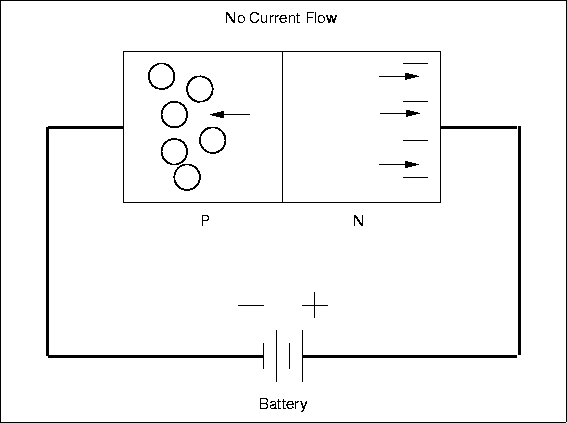
If the polarity of the applied voltage is reversed, then the diode will be reverse biased and will appear nonconducting (Fig. 4.14). Almost no current will flow and there will be a large voltage across the device.
  
Figure 4.14: A Reverse Biased Diode
\begin{figure}

\fbox {\centerline{\psfig{figure=basicelec/rbdiode.PS}}}\end{figure}

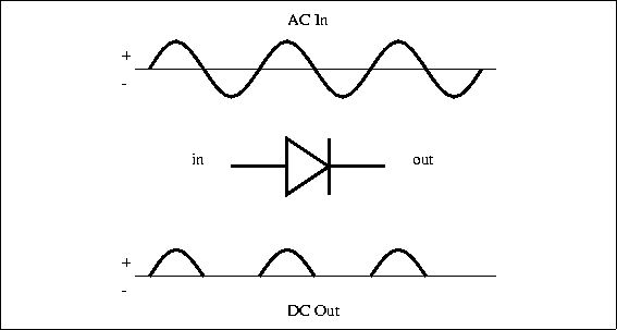
The non-symmetric behavior is due to the detailed properties of the pn-junction. The diode acts like a one-way valve for current and this is a very useful characteristic. One application is to convert alternating current (AC), which changes polarity periodically, into direct current (DC), which always has the same polarity. Normal household power is AC while batteries provide DC, and converting from AC to DC is called rectification. Diodes are used so commonly for this purpose that they are sometimes called rectifiers, although there are other types of rectifying devices. Figure 4.15 shows the input and output current for a simple half-wave
  
Figure 4.15: A Half-Wave Rectifier
\begin{figure}

\fbox {\centerline{\psfig{figure=basicelec/halfrect.PS}}}\end{figure}

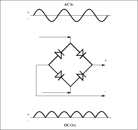
rectifier. The circuits gets its name from the fact that the output is just the positive half of the input waveform. A full-wave rectifier circuit (shown in Figure 4.16) uses four diodes arranged so that both polarities of the input waveform can be used at the output.
  
Figure 4.16: A Full-Wave Rectifier
\begin{figure}

\fbox {\centerline{\psfig{figure=basicelec/fullrect.PS}}}\end{figure}


The full-wave circuit is more efficient than the half-wave one.

Silicon


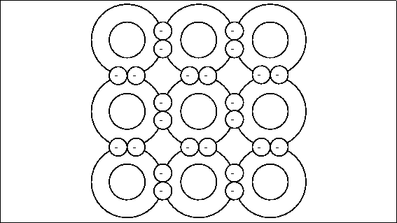
Semiconductor devices are made primarily of silicon (silicon's element symbol is "Si"). Pure silicon forms rigid crystals because of its four valence (outermost) electron structure -- one Si  atom bonds to four other Si atoms forming a very regularly shaped diamond pattern. Figure 4.10 shows part of a silicon crystal structure.
  
Figure 4.10: A Silicon Crystal Structure
\begin{figure}

\fbox {\centerline{\psfig{figure=basicelec/silicon.PS}}}\end{figure}

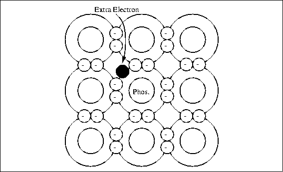
Pure silicon is not a conductor because there are no free electrons; all the electrons are tightly bound to neighboring atoms. To make silicon conducting, producers combine or "dope" pure silicon with very small amounts of other elements like boron or phosphorus. Phosphorus has five outer valence electrons. When three silicon atoms and one phosphorus atom bind together in the basic silicon crystal cell of four atoms, there is an extra electron and a net negative charge. Figure4.11 shows the crystal structure of phosphorus doped silicon.
  
Figure 4.11: Silicon Doped with Phosphorus
\begin{figure}

\fbox {\centerline{\psfig{figure=basicelec/phosphorus.PS}}}\end{figure}

This type of material is called n-type silicon. The extra electron in the crystal cell is not strongly attached and can be released by normal thermal energy to carry current; the conductivity depends on the amount of phosphorus added to the silicon.
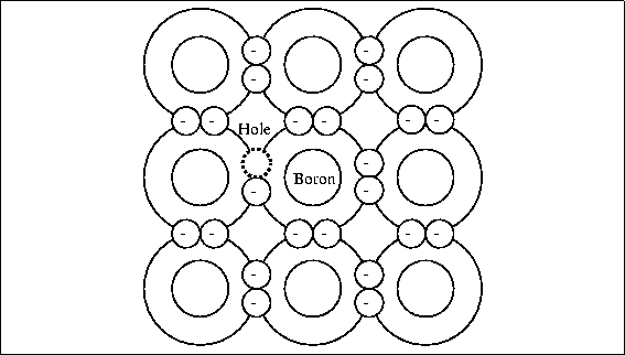
Boron has only three valance electrons. When three silicon atoms and one boron atom bind with each other there is a "hole" where another electron would be if the boron atom were silicon; see Fig. 4.12. This gives the crystal cell a positive net charge (referred to as p-type silicon), and the ability to pick up an electron easily from a neighboring cell.
  
Figure 4.12: Silicon Doped with Boron
\begin{figure}

\fbox {\centerline{\psfig{figure=basicelec/boron.PS}}}\end{figure}


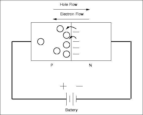
The resulting migration of electron vacancies or holes acts like a flow of positive charge through the crystal and can support a current. It is sometimes convenient to refer to this current as a flow of positive holes, but in fact the current is really the result of electrons moving in the opposite direction from vacancy to vacancy.

Semiconductor Devices

The Truth About Charge   

Our statements above about charge are not wrong, but they are simple and incomplete. In order to understand how semiconductor devices work one needs a more complete description of the nature of charge in the real world. Charge does not exist independently; it is carried by subatomic particles. For this discussion we will be concerned primarily with electrons, which carry a negative charge of 1.6  10-19 C , the minimum amount of charge that can exist in isolation. At least, no one has found any smaller amount than this fundamental quantum of charge.
Electrons are one component of atoms and molecules. Atoms are the building blocks out of which all matter is constructed. Atoms bond with each other to form substances. Substances composed of just one type of atom are called elements. For example, copper, gold and silver are all elements; that is, each of them consists of only one type of atom. More complex substances are made up of more than one atom and are known as compounds. Water, which has both hydrogen and oxygen atoms, is such a compound. The smallest unit of a compound is a molecule. A water molecule, for example, contains two hydrogen atoms and one oxygen atom.
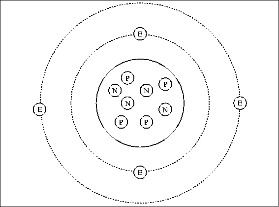
Atoms themselves are made up of even smaller components: protonsneutrons and electrons. Protons and neutrons form the nucleus of an atom, while the electrons orbit the nucleus. Protons carry positive charge and electrons carry negative charge; the magnitude of the charge for both particles is the same, one quantum charge, 1.6 �10-19 C . Neutrons are not charged. Normally, atoms have the same number of protons and electrons and have no net electrical charge.

  
Figure 4.8: Structure of an Atom
\begin{figure}

\fbox {\centerline{\psfig{figure=basicelec/atomstruct.PS}}}\end{figure}

Electrons that are far from the nucleus are relatively free to move around under the influence of external fields because the force of attraction from the positive charge in the nucleus is weak at large distances. In fact, it takes little force in many cases to completely remove an outer electron from an atom, leaving an ion with a net positive charge. Once free, electrons can move at speeds approaching the speed of light (roughly 670 million miles per hour) through metals, gases and vacuum. They can also become attached to another atom, forming an ion with net negative charge.
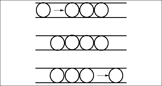
Electric current in metal conductors consists of a flow of free electrons. Because electrons have negative charge, the flow of electrons is in a direction opposite to the positive current. Free electrons traveling through a conductor drift until they hit other electrons attached to atoms. These electrons are then dislodged from their orbits and replaced by the formerly free electrons. The newly freed electrons then start the process anew. At the microscopic level, electron flow through a conductor is not a steady stream, like water flowing from a faucet, but rather a series of short bursts.

  
Figure 4.9: A Simple Model of Electron Flow
\begin{figure}

\fbox {\centerline{\psfig{figure=basicelec/eflow.PS}}}\end{figure}

Batteries

Batteries    

Charges can be separated by several means to produce a voltage. A battery uses a chemical reaction to produce energy and separate opposite sign charges onto its two terminals. As the charge is drawn off by an external circuit, doing work and finally returning to the opposite terminal, more chemicals in the battery react to restore the charge difference and the voltage. The particular type of chemical reaction used determines the voltage of the battery, but for most commercial batteries the voltage is about 1.5 V per chemical section or cell. Batteries with higher voltages really contain multiple cells inside connected together in series. Now you know why there are 3 V, 6 V, 9 V, and 12 V batteries, but no 4 or 7 V batteries. The current a battery can supply depends on the speed of the chemical reaction supplying charge, which in turn often depends on the physical size of the cell and the surface area of the electrodes. The size of a battery also limits the amount of chemical reactants stored. During use, the chemical reactants are depleted and eventually the voltage drops and the current stops. Even with no current flow, the chemical reaction proceeds at a very slow rate (and there is some internal current flow), so a battery has a finite storage or shelf life, about a year or two in most cases. In some types of batteries, like the ones we use for the robot, the chemical reaction is reversible: applying an external voltage and forcing a current through the battery, which requires work, reverses the chemical reaction and restores most, but not all, the chemical reactants. This cycle can be repeated many times. Batteries are specified in terms of their terminal voltage, the maximum current they can deliver, and the total current capacity in ampere-hours.
You should handle batteries carefully, especially the ones we use in this course. Chemicals are a very efficient and compact way of storing energy. Just consider the power of gasoline or explosives, or the fact that you can play soccer for several hours powered only by a slice of cold pizza for breakfast. Never connect the terminals of a battery together with a wire or other good conductor. The battery we use for the RoboBoard is similar to the battery in cars, which uses lead and sulphuric acid as reactants. Such batteries can deliver very large currents through a short circuit, hundreds of  amperes. The large current will heat the wire and possibly burn you; the resulting rapid internal chemical reactions also produce heat and the battery can explode, spreading nasty, reactive chemicals about. Charging these batteries with too large a current can have the same effect. Double check the circuit and instructions before connecting a battery to any circuit.